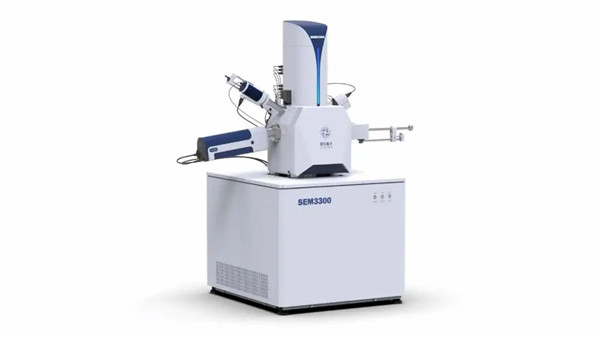
State-of-the-art electron microscope debuts in Hefei
Updated: 2022-11-29
|chinadaily.com.cn
The first commercial tungsten filament scanning electron microscope or SEM in the world with a resolution of 2.5 nanometers recently debuted in Hefei city, capital of East China's Anhui province.
It was launched on Nov 24 by Hefei-based scientific instruments developer Chinainstru & Quantumtech (Hefei) Co Ltd, or CIQTEK.

CIQTEK's cutting-edge SEM 3300. [Photo/WeChat ID: hefeigaoxinfabu]
By using the interaction between electrons and substance, electron microscopes can obtain various physical and chemical properties of a sample itself, such as its morphology, composition and structure. It is said to be a powerful tool for materials research, quality control and failure analysis.
Tungsten filament SEMs are widely used because they are cost-effective and easy to maintain and operate. However, the resolutions of tungsten filament SEMs were considered less than optimal, and it was difficult to meet the increasing needs of users for higher resolutions.
CIQTEK's quantum technology team carried out extensive research to solve this technical bottleneck and it came up with a solution. The SEM 3300's resolution, which is 2.5 nm at 20 kV, is 16 percent higher than that of conventional tungsten filament electron microscopes and is said to have outstanding resolutions at any other voltages.
CIQTEK also launched its SEM2000, which is super easy to operate, and a field emissions SEM 4000, a new product for analytical users.
